Franz Selbmann and Frank Roscher, Fraunhofer Institute for Elektronic Nano Systems ENAS
Parylene based Technologies for smart coatings and wearables
Considering ongoing trends such as the „Internet of Things“ and „Smart Everything“, the integration of functional elements like sensors and actuators in items of daily use is necessary to enable new features. A promising approach for this is the fabrication of electronic systems by embedding active and passive electronic components into polymer coatings, using established technologies for layer deposition.
A polymer, which is established in the coating technology and which combines various excellent properties is Parylene. Beside its chemical inertness, optical transparency, good temperature stability, low permeability and dielectric properties, in particular its ISO 10993 certified biocompatibility and biostability are of high interest for numerous applications. In addition, its deposition process at room temperature is advantageous and enables the coating of various materials such as printed circuit boards, wafers or paper. The resulting layers are highly conformal and without internal stresses. Typical layer thicknesses are in the range of several micrometers only. For the integration of different functional elements, the realization of miniaturized metallic conductive pathes as well as their embedding into Parylene are crucial.
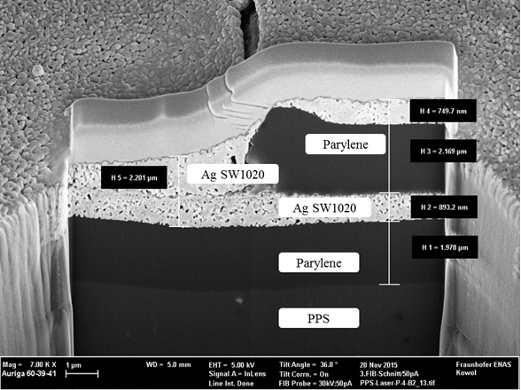
Based on microtechnological processes, the realization of different metallic structures was established on and in Parylene at Fraunhofer ENAS. Using sputtering processes with subsequent patterning by lithography and wet-chemical etching, resolutions down to 5 µm were demonstrated for metals such as Gold, Aluminum, Titanium, Chrome and Copper. Furthermore, additive technologies such as screen printing or aerosol jet printing can be used for the patterned deposition of silver inks and pastes. Using dry etching and laser ablation of Parylene, even layouts with several metallization layers can be realized. E. g. in Fig. 1 the cross-section of a Parylene coated Polyphenylene sulfide (PPS) is imaged with two integrated metallization layers of silver conductive paths printed by aerosol jet. These two metallization layers are electrically connected by a through-hole contact.
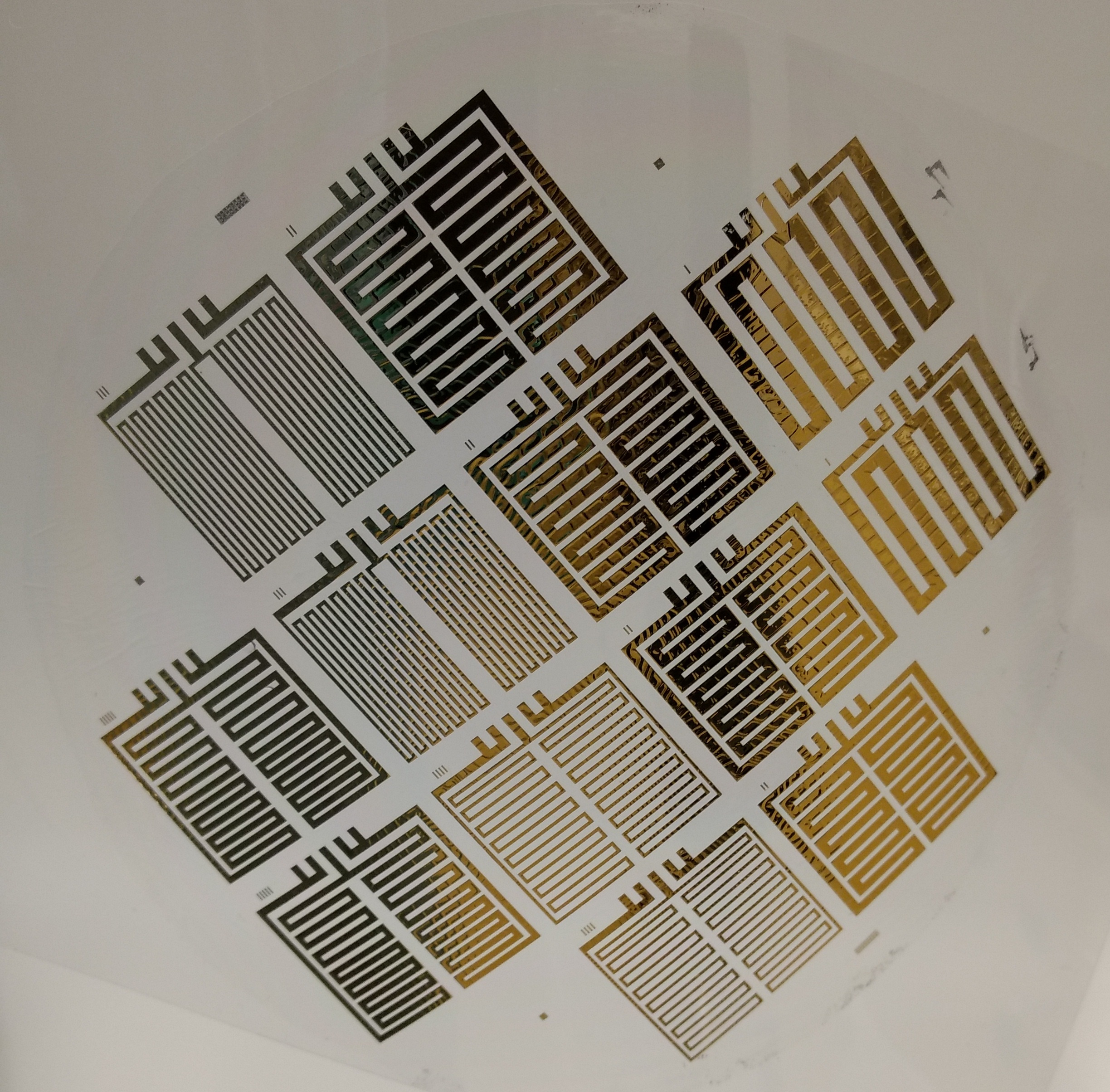
In addition to the described metallization technologies, a process for the realization of free-standing Parylene foils was developed. This enables the usage of Parylene as a substrate for wearables. Fig. 2 depicts a free-standing Parylene substrate with gold structures. Besides conductive paths also sensors can be realized, e. g. for temperature or strain. In future, the obtained flexible electronic systems can be attached conformally to complex geometries.
In summary, using Parylene either as a coating material or a free-standing substrate and in combination with different metallization technologies enables various applications for smart coatings and wearables.
 Fraunhofer-Gesellschaft
